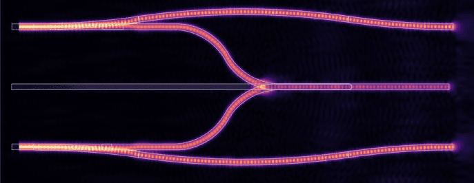
Tarranix develops its first guided-wave Toffoli gate using beam interference
A significant step toward fully optical logical circuits based on reversible photonic computing.
READ MORE
By Tarranix
Technology
As a part of the ongoing development of the revolutionary Tarranix photonic chip, our team has successfully completed initial simulations using a cross-shaped photonic crystal (PhC Cross) structure. These results confirm the design's potential for precisely guiding and controlling light propagation at the nanoscale- an essential requirement for enabling six-state optical logic.
The simulations were conducted using advanced FDTD (Finite Difference Time Domain) methods, focusing on electromagnetic field dynamics within optimized photonic structures for optical switching. The results show high field localization and coherent transmission, validating the theoretical foundation of multilevel photonic transistors.
Below are two images from the simulations showing the electric field dynamics for E and Ez:
The PhC simulation demonstrates how the design of strategic defects - such as waveguides and precisely placed holes- guide light through the structure. It can be seen that, although te incident light is in TE mode (Transvers Electric ), the arrangement of the holes modifies the photonic band structure, enabling light to propagate in the Z direction at the intersection of the two light beams. This effect is crucial for the development of optical logic gates capable of encoding multiple polarization states.
A significant step toward fully optical logical circuits based on reversible photonic computing.
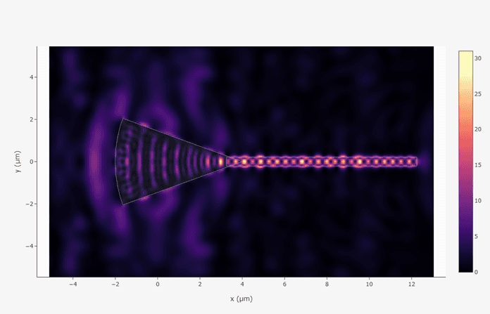
Tarranix developed a 6 µm vertical grating coupler for 3D photonic interconnections. Si/SiO₂ simulations show efficient light coupling. A Si₃N₄ version is in progress to enhance performance.
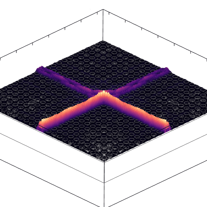
Tarranix has completed the first design phase of a photonic crystal (PhC) transistor with out-of-plane emission, adapted to the fabrication capabilities of UPC.