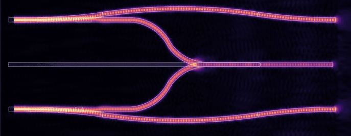
Tarranix develops its first guided-wave Toffoli gate using beam interference
A significant step toward fully optical logical circuits based on reversible photonic computing.
READ MORE
By Tarranix
Technology
Tarranix (Brainlab Fira) has completed the first phase of design for fabrication of a photonic crystal (PhC) transistor featuring out-of-plane (z-axis) light emission.
The design has been adjusted to the parameters dictated by the lithography and etching capabilities available on UPC machinery. In parallel, the electromagnetic simulations have been expanded with a realistic layer stack and process considerations: substrate and oxides (BOX), guiding layer (SiN/Si, depending on the variant). The model incorporates material losses, PML boundary conditions, and a sensitivity analysis (variations in hole radius, period, and thickness) so that the design faithfully reflects fabrication and measurement conditions.
Compliance with general design rules has been verified in KLayout using the SiEPIC DRC, and the simulations confirm the intended symmetry breaking and the redirection of light.
The lateral view of the simulation field maps are shown in the GIF above. The distribution confirms symmetry breaking and the redirection of light towards the z-axis.
The project will now focus on verifying and finalizing the design according to the specific parameters of UPC machinery (e.g., overlay, etch anisotropy, sidewall roughness, and film thickness/stress) to consolidate the mask set for the fabrication and characterization of the first real device.
A significant step toward fully optical logical circuits based on reversible photonic computing.
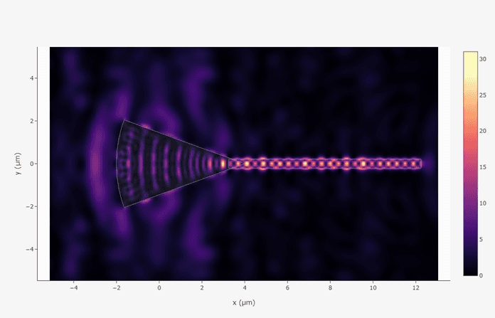
Tarranix developed a 6 µm vertical grating coupler for 3D photonic interconnections. Si/SiO₂ simulations show efficient light coupling. A Si₃N₄ version is in progress to enhance performance.
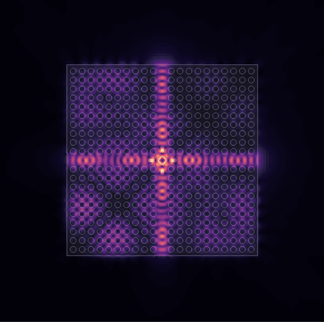
The Tarranix project has successfully completed simulations using a photonic crystal cross structure, making a key step in the development of optical logic with six logical states per transistor.