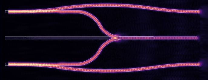
Tarranix develops its first guided-wave Toffoli gate using beam interference
A significant step toward fully optical logical circuits based on reversible photonic computing.
READ MORE
By Tarranix
Highlights
Tarranix has officially received certification from the Agencia de Certificación e Innovación Empresarial (ACIE), an important step in validating the technological and industrial feasibility of our photonic computing technology. This certification confirms that our research, prototyping, and system integration meet industry standards for efficiency, scalability, and technical soundness.
The certification process involved evaluating key performance indicators in our three-dimensional photonic chip, which integrates multi-state optical transistors to explore new computing paradigms beyond traditional silicon-based architectures.
The ACIE certification is awarded after a rigorous assessment of a technology’s feasibility, innovation level, and potential for industrial application. Through this certification, Tarranix has demonstrated:
Computational efficiency, by testing photonic logic gates and transistors with multi-state light polarization techniques.
Energy consumption advantages, showing the potential for lower power requirements compared to conventional silicon chips.
Scalability considerations, ensuring that the technology is compatible with manufacturing processes for further development.
Technical validation, confirming that the project aligns with industry expectations for emerging semiconductor technologies.
Receiving ACIE certification represents a step forward in the continued research, testing, and potential industrialization of our photonic computing technology. While this certification does not yet signify mass-market readiness, it validates the technical feasibility of our work and supports future efforts in commercial scaling and partnership development.
Following ACIE’s certification, Tarranix is focused on:
Further development and optimization of our photonic chip technology through additional testing and refinement.
Expanding collaboration efforts with research institutions, semiconductor manufacturers, and technology firms.
Exploring industrial applications for photonic computing, including AI acceleration and data-intensive processing.
Filing intellectual property protections to safeguard advancements in optical transistor research.
The ACIE certification marks a significant milestone in our project, reinforcing the scientific and technical foundation of our photonic chip development. As research progresses, we remain committed to transparency and collaboration in shaping the potential role of photonic computing in future semiconductor applications.
Stay connected for further updates as Tarranix continues its research and development in next-generation computing architectures.
A significant step toward fully optical logical circuits based on reversible photonic computing.
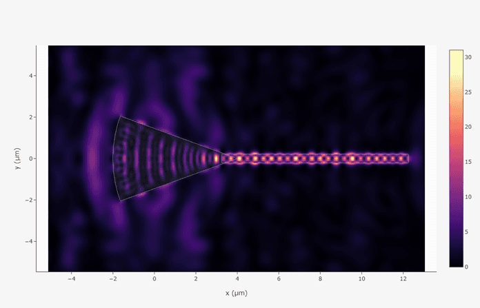
Tarranix developed a 6 µm vertical grating coupler for 3D photonic interconnections. Si/SiO₂ simulations show efficient light coupling. A Si₃N₄ version is in progress to enhance performance.
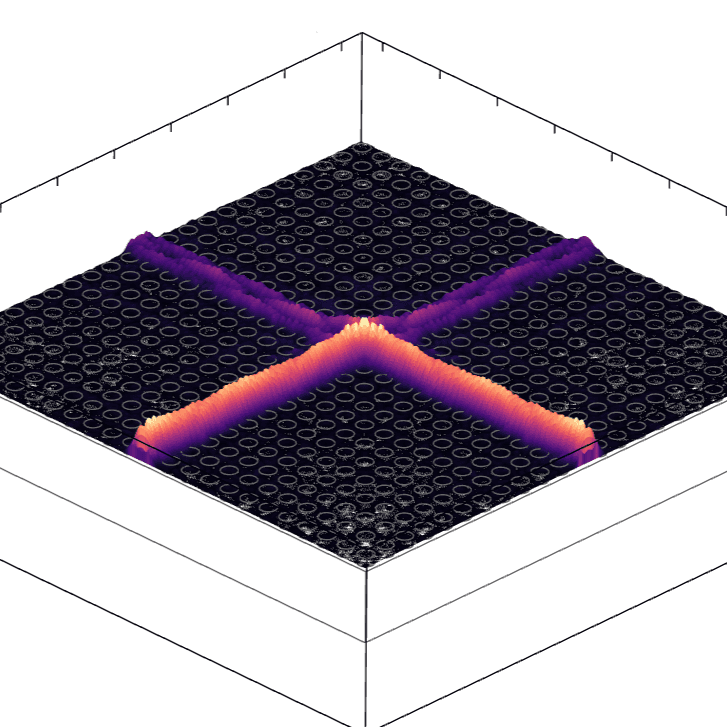
Tarranix has completed the first design phase of a photonic crystal (PhC) transistor with out-of-plane emission, adapted to the fabrication capabilities of UPC.