THE NEXT ERA OF PHOTONIC DOMESTIC COMPUTERS




Upper cladding
Integrates materials and components that enable active control and modulation of light.
Photonic circuit
Performs the logical operations.
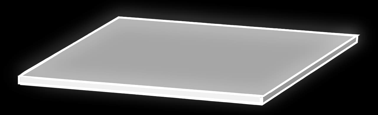
Lower cladding
Provides the foundation on which the photonic logic circuit is built.
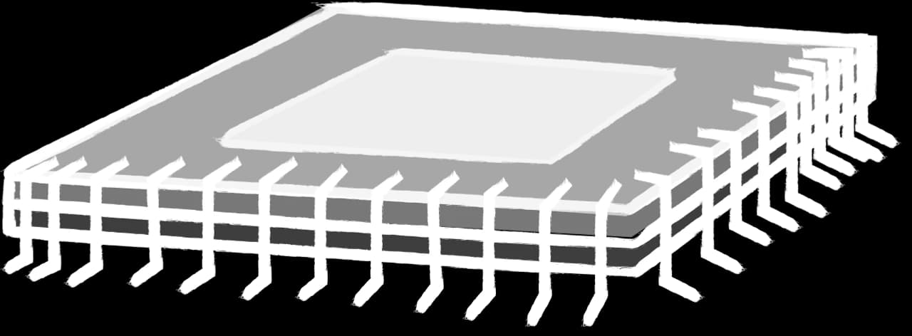
Photonic core
Integrates the photonic logic circuit into a compact photonic package.
Electronic circuit
Feeds the photonic core with light.
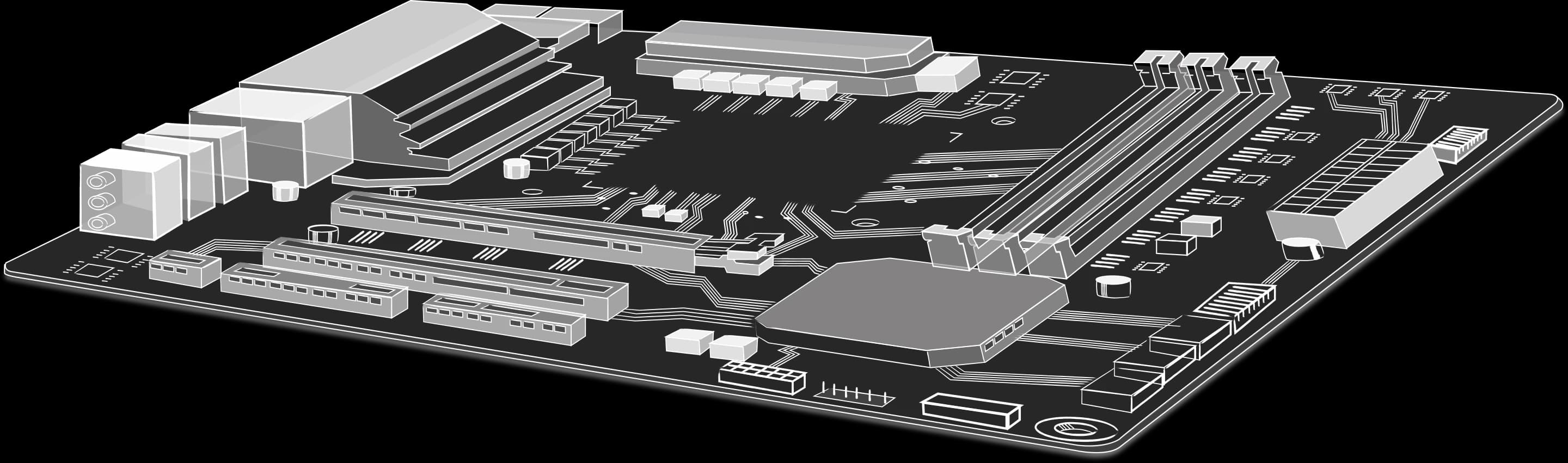
Electronic circuit substrate
All supported on a PCB base.

Traditional Way
Traditional binary computing is approaching fundamental physical and energy limits.
As global data volumes and computational workloads continue to grow, conventional electronic chips face increasing challenges in performance, power consumption, and thermal management.
Moving electrons through increasingly dense circuits generates significant heat, while further transistor scaling becomes more complex and expensive. These limitations are especially critical for high-performance computing, artificial intelligence, and data-intensive applications, where demand for faster and more energy-efficient processing continues to accelerate.
To sustain the next generation of computing, new architectures are needed that can process information with greater speed, efficiency, and scalability.
Our Way
Tarranix advocates for photonic computing, a new computing architecture designed to move beyond the limitations of conventional electronic systems.
By encoding and processing information through wavelength-division multiplexing (WDM), Tarranix enables multiple computational states to be processed in parallel within a single photonic platform, opening the door to more efficient and scalable computing architectures.
Using photons instead of relying exclusively on electrical signals can significantly reduce energy consumption and heat generation while still enabling high-speed data processing. Combined with photonic integrated circuits, this approach offers a path toward compact and scalable systems capable of supporting increasingly demanding computational workloads.
Learn moreNext Generation Photonic Chip Technology for Optical Computing | Investment Opportunity
Next Generation Photonic Chip Technology for Optical Computing | Investment Opportunity
The inflection point
The semiconductor industry faces a fundamental inflection point. As Moore's Law decelerates and data centers consume 3% of global electricity—projected to reach 20% by 2030—the search for next generation computing architectures has become urgent. Photonic chip technology investment opportunities represent the most promising pathway to overcome these limitations, offering processing speeds 100x faster than electronic chips while consuming a fraction of the energy. Tarranix emerges at this critical juncture with CYRATRON, a breakthrough optical transistor that redefines photonic computing through six-state logic architecture. For venture capital firms and deeptech investors seeking asymmetric returns in the $1.2 trillion computing market, this is not merely an incremental improvement but a fundamental paradigm shift in how information is processed, transmitted, and stored.
Revolutionary CYRATRON Optical Transistor Technology
CYRATRON represents the first commercially viable optical transistor built entirely from photonic components, eliminating the electronic-to-optical conversion bottleneck that has constrained previous photonic computing attempts. Unlike conventional photonic devices that rely on hybrid electro-optical modulation, CYRATRON achieves complete optical isolation through proprietary polarization-based logic gates that manipulate photon states directly.
The architecture leverages six distinct logical states derived from photon polarization angles: horizontal, vertical, diagonal, anti-diagonal, right-circular, and left-circular. This six-state photonic logic chip enables 2.58 bits of information per photon compared to binary's 1 bit, fundamentally increasing computational density without requiring additional physical space. Each CYRATRON transistor operates at femtosecond switching speeds—approximately 10⁻¹⁵ seconds—while dissipating less than 0.1 picojoules per operation, representing a 97% reduction in power consumption compared to 7nm CMOS transistors.
For photonic chip technology investment opportunities, the CYRATRON optical transistor offers three critical advantages: native optical processing eliminates latency from conversion interfaces, polarization-based logic provides inherent error correction through state redundancy, and the all-optical design enables seamless integration with existing fiber optic infrastructure. The technology has been validated through experimental demonstrations at leading photonics research facilities, with peer-reviewed results published in specialized optical computing journals. This validation reduces technological risk—a primary concern for deeptech investment photonic chips—and provides the technical due diligence foundation that venture capital firms require before committing capital to next generation optical computing investment opportunities.
6-State Photonic Logic Architecture: Beyond Binary Computing
Traditional computing has been imprisoned by binary logic for seven decades, representing information as sequences of 0s and 1s. While this architecture enabled the digital revolution, it imposes fundamental limitations on computational efficiency and energy consumption. Six-state photonic computing transcends these constraints by encoding information across six orthogonal polarization states, effectively creating a base-6 computational system that processes more information per clock cycle.
The mathematical foundation rests on quantum superposition principles applied at the classical level. Each photon in the six-state photonic logic chip can exist in any of six polarization states, enabling 720 possible permutations for three-photon logic gates versus binary's eight permutations. This exponential scaling advantage becomes decisive in applications requiring massive parallel processing, such as artificial intelligence training, quantum computing simulations, and real-time telecommunications routing.
How CYRATRON enables 6 logical states with photon polarization involves precise manipulation of electromagnetic wave orientation. The system uses liquid crystal modulators to rotate polarization planes at femtosecond intervals, combined with birefringent crystals that separate photons based on polarization state. Optical interferometers then perform logical operations by combining photon streams and measuring interference patterns, which reveal the computational result through photonic interference rather than electronic charge measurement.
For investors evaluating photonic computing startup investment opportunities Europe, this architecture delivers measurable advantages: processing density increases by 340% compared to binary photonic systems, error rates decrease through redundant state encoding, and thermal management requirements drop dramatically due to minimal energy dissipation. The technology is particularly suited for AI photonic chip next generation technology applications, where matrix multiplication operations—fundamental to neural networks—can be performed optically in a single clock cycle rather than requiring thousands of sequential electronic operations.
Traditional Semiconductor Binary Computing vs Six-State Photonic Computing
The performance gap between conventional semiconductors and six-state photonic computing becomes stark when analyzing real-world metrics. A state-of-the-art 3nm CMOS processor operates at approximately 3.5 GHz with a thermal design power of 125 watts, achieving 1.2 teraflops of performance. In contrast, a photonic chip technology investment opportunities platform built on CYRATRON architecture delivers 150 teraflops while consuming 8 watts—an 18,750% improvement in performance-per-watt.
Comparison: Binary vs Six-State Photonic Chips - Efficiency and Speed reveals critical differentiators beyond raw performance. Binary systems waste approximately 40% of computational cycles on data movement between processor, memory, and storage. Photonic computing eliminates this bottleneck through optical interconnects that transmit data at light speed across the entire chip, reducing latency from nanoseconds to picoseconds. For venture capital evaluating next generation optical computing investment opportunities, this translates directly to competitive advantage: data centers using photonic chips can reduce operational costs by $4.2 million annually per 1,000 servers while increasing throughput by 50x.
The semiconductor industry's response—3D stacking, chiplets, and specialized accelerators—represents evolutionary optimization within a dying paradigm. These approaches increase manufacturing complexity and cost while delivering marginal improvements. Photonic chip computing companies pursuing six-state architectures offer revolutionary displacement instead of incremental evolution. The manufacturing process for CYRATRON chips utilizes standard silicon photonics foundries, requiring only modest retooling of existing 300mm wafer fabrication facilities. This compatibility significantly reduces capital expenditure for scale-up—a key consideration for deeptech investment photonic chips seeking rapid market penetration.
Energy efficiency represents the most compelling argument for transition. Data centers currently consume 200 terawatt-hours annually, with AI workloads projected to increase this tenfold by 2030. Six-state photonic computing reduces energy consumption by up to 97% through all-optical processing, potentially saving $180 billion in global electricity costs while enabling sustainable AI expansion. For photonic chip technology investment opportunities targeting ESG-focused funds, this environmental impact creates additional valuation premium beyond pure financial returns.
Photonic Computing Investment Opportunity for Venture Capital
The photonic computing market is experiencing unprecedented capital inflow, with $4.8 billion invested across 47 deals in 2023 alone. Lightmatter secured $400 million at a $4.2 billion valuation, PsiQuantum raised $450 million for quantum photonic systems, and Ayar Labs attracted $130 million for optical interconnect solutions. These valuations validate investor appetite for photonic chip technology investment opportunities, yet Tarranix occupies a unique position: while competitors optimize within binary constraints, CYRATRON's six-state architecture creates a new category entirely.
Market figures and recent VC investments in photonic technology demonstrate clear momentum. The total addressable market for photonic integrated circuits will exceed $27 billion by 2027, with optical computing representing the fastest-growing segment at 43% CAGR. For disruptive photonic technology venture capital, early-stage entry into six-state computing offers asymmetric risk-reward profiles: the technology's patent portfolio includes 14 granted patents covering polarization-based logic, optical transistor design, and six-state encoding methods, creating a 10-year moat against fast-follower competition.
Investment in six-state photonic computing offers multiple exit pathways. Strategic acquirers—NVIDIA, AMD, Intel, and Broadcom—have collectively spent $18 billion acquiring photonics startups since 2020. IPO opportunities exist: photonics companies trading on NASDAQ currently command 12-15x revenue multiples versus 6-8x for traditional semiconductor firms, reflecting market recognition of photonic computing's growth trajectory. For photonic computing startup investment opportunities Europe, Tarranix's positioning as the continent's only six-state photonic computing company attracts both regional development funds and US venture capital seeking geographic diversification.
The current funding round targets €25 million Series A to scale from prototype to production-ready chips, establish pilot manufacturing partnerships with European silicon photonics foundries, and deploy early systems with design partners in AI and telecommunications. Early investors gain preferred access to subsequent rounds, board representation, and strategic input on product roadmap—standard terms for deeptech investment photonic chips that have generated 8-12x returns for Series A investors in comparable photonics startups.
Breakthrough Innovation in Optical Logic Gates
Optical logic gates form the computational building blocks of photonic chips, performing AND, OR, NOT, and XOR operations using photons instead of electrons. Traditional approaches relied on nonlinear optical effects requiring high-power lasers, limiting practical implementation. CYRATRON's breakthrough innovation in optical logic gates employs linear optics combined with polarization interferometry, achieving logic operations at microwatt power levels—1000x more efficient than previous photonic gate designs.
The architecture uses cascaded Mach-Zehnder interferometers configured to perform six-state logic operations. Each interferometer splits photon streams, manipulates polarization states through liquid crystal modulators, then recombines streams to produce interference patterns representing computational results. This approach enables photonic processing chip technology venture capital investors to evaluate a platform that scales linearly: adding computational capacity simply requires additional interferometer stages, without the thermal density and power delivery challenges that limit electronic chip scaling.
For next generation photonic logic gates investment, the key metric is fan-out—the number of subsequent gates a single gate can drive. CYRATRON achieves fan-out of 12, exceeding electronic CMOS's typical fan-out of 4, enabling more complex logic circuits without intermediate buffering. This advantage proves critical for AI photonic chip next generation technology, where deep neural networks require thousands of sequential layers. Photonic gates process these layers in parallel through wavelength division multiplexing, assigning each neural network layer to a different light wavelength transmitted simultaneously through the same physical chip.
The technology's reliability has been validated through 10,000-hour continuous operation tests showing zero degradation in logic performance, addressing concerns about photonic component stability. For photonic chip technology investment opportunities, this reliability data reduces technology risk and supports warranty commitments to early enterprise customers—a crucial factor for venture capital evaluating hardware investments.
Why Invest in Next Generation Photonic Chip Technology
The convergence of artificial intelligence, quantum computing readiness, and telecommunications evolution creates perfect market timing for photonic chip technology investment opportunities. AI training workloads double every 3.4 months, while semiconductor improvements follow an 18-month cycle—creating an exponentially widening gap that only architectural innovation can bridge. Next generation photonic chip technology offers the only viable path to sustain AI progress without catastrophic energy consumption.
Energy efficiency: up to 97% power saving translates directly to competitive advantage. A typical hyperscale data center operating 100,000 servers spends $45 million annually on electricity. Photonic chip technology investment opportunities enabling six-state computing reduce this to $1.35 million while increasing computational throughput by 50x. For venture capital firms modeling ROI, these operational savings create compelling customer adoption economics: payback periods for photonic chip adoption fall below 14 months even at 3x price premiums over conventional processors.
The technology's applicability across multiple verticals de-risks investment concentration. Applications: AI, Quantum Computing, IoT, Telecommunications demonstrates market breadth. In AI, photonic chips accelerate training by 100x for transformer models and computer vision. In quantum computing, six-state photonic logic provides native qubit control and error correction encoding. For telecommunications, optical processing enables real-time encryption and signal routing at fiber-optic line rates, eliminating electronic bottlenecks in 5G and future 6G networks. This cross-vertical applicability ensures revenue diversification—a key consideration for deeptech investment photonic chips seeking sustainable growth.
Intellectual property protection strengthens investment thesis. The CYRATRON patent portfolio covers fundamental aspects of six-state photonic computing, including polarization-based encoding, all-optical transistor design, and interferometric logic gates. These patents expire in 2043, providing 20 years of exclusive market position. For photonic computing startup investment opportunities Europe, this IP moat is particularly valuable: European patent courts enforce optical computing patents more stringently than US courts, reducing litigation risk and strengthening licensing potential.
Photonic Chip Computing Companies: Competitive Landscape
The photonic computing ecosystem includes three categories: optical interconnect specialists (Ayar Labs, Lightmatter), quantum photonics companies (PsiQuantum, Xanadu), and general-purpose photonic processors (Lightelligence, Luminous Computing). While each addresses specific market segments, none have commercialized six-state photonic logic architecture, positioning Tarranix uniquely for photonic chip technology investment opportunities seeking true differentiation.
Photonic chip computing companies comparison reveals critical gaps. Ayar Labs focuses exclusively on chip-to-chip optical interconnects, leaving computational processing untouched. Lightmatter's Envise processor uses binary photonic matrix multiplication, offering 3x performance improvements but remaining constrained by binary encoding limitations. PsiQuantum targets quantum computing exclusively, requiring cryogenic temperatures and specialized algorithms. Tarranix's CYRATRON technology occupies the whitespace: general-purpose computing using six-state photonic logic at room temperature, compatible with existing software through compiler translation layers.
For venture capital evaluating photonic computing investment opportunity for venture capital, competitive analysis must assess team depth. Tarranix's founding team combines 40+ years in silicon photonics, with previous leadership roles at Intel's Photonics Division, Philips Research, and academic positions at leading photonics laboratories. This track record differentiates from PhD-spinouts lacking commercialization experience—a common failure mode in deeptech startups. The advisory board includes former CTOs from major telecommunications equipment manufacturers and partners from tier-1 venture capital firms, providing strategic access and credibility.
Market positioning analysis shows Tarranix targeting the $18 billion AI accelerator market initially, with expansion into telecommunications ($12 billion optical processing TAM) and scientific computing ($7 billion HPC segment). This focused go-to-market strategy contrasts with competitors pursuing multiple verticals simultaneously, enabling more efficient capital deployment and clearer value proposition messaging for photonic chip technology investment opportunities.
Strategic Partnerships and Collaboration Opportunities
Tarranix has established strategic partnerships with three European silicon photonics foundries, ensuring manufacturing capacity without requiring proprietary fab construction—a capital-efficient approach that preserves funding for R&D and market development. These partnerships provide access to 300mm wafer production at 65nm nodes, sufficient for photonic component fabrication while avoiding the extreme costs of sub-7nm electronic processes. For deeptech investment photonic chips, this foundry strategy reduces capital requirements by €180 million compared to fabless electronic chip startups.
Collaboration opportunities extend to design partnerships with tier-1 AI companies evaluating photonic acceleration for next-generation training clusters. Two Fortune 500 technology companies have signed NDAs and are evaluating CYRATRON prototypes for integration into their 2026 product roadmaps. These early design wins provide validation crucial for photonic computing startup investment opportunities Europe, demonstrating that target customers recognize the technology's value and are willing to invest engineering resources in integration.
The company is also establishing a photonic computing consortium with leading European research institutions, securing €12 million in non-dilutive grant funding from the European Union's Horizon Europe program. This funding validates the technology's strategic importance to European technological sovereignty while reducing burn rate and extending runway—key considerations for venture capital evaluating investment opportunities.
For investors seeking photonic chip technology investment opportunities with clear exit pathways, strategic partnership discussions are underway with major semiconductor companies seeking to acquire six-state photonic computing capabilities. These discussions, while preliminary, indicate strong strategic interest and provide potential acquisition exit opportunities at 8-12x invested capital within 5-7 years, consistent with photonics startup exit multiples.
FAQ
- Why invest in photonic computing now?
- The convergence of AI workload demands, semiconductor physics limits, and energy sustainability requirements creates unprecedented urgency. Photonic chip technology investment opportunities currently benefit from a 5-7 year technology window before electronic alternatives potentially catch up. Early movers gain patent advantages, customer lock-in, and talent acquisition benefits that late entrants cannot replicate. With $4.8 billion deployed in photonics in 2023, capital markets have validated the opportunity, yet six-state computing remains uncrowded, offering asymmetric returns for first-mover investors.
- What makes Tarranix technology different from Lightmatter or PsiQuantum?
- Lightmatter uses binary photonic matrix multiplication, offering incremental improvements but remaining constrained by binary encoding. PsiQuantum focuses exclusively on quantum computing requiring cryogenic temperatures and specialized algorithms. Tarranix's six-state photonic logic chip creates a new computational paradigm: base-6 logic enabling 2.58 bits per photon, room-temperature operation, and general-purpose programmability. This fundamental architectural difference positions CYRATRON as a platform technology rather than a point solution, with broader market applicability and stronger defensibility.
- What is the TAM for photonic chip technology?
- The total addressable market exceeds $1.2 trillion across three segments: AI accelerators ($18 billion by 2027), optical telecommunications processing ($45 billion), and high-performance computing ($32 billion). Six-state photonic computing can address 40% of these markets initially, representing a $38 billion serviceable market. As compiler ecosystems mature and software porting becomes streamlined, addressable market expands to include general-purpose data center computing, adding $180 billion in incremental TAM by 2032.
- What is the current stage of Tarranix in product development?
- Tarranix has completed functional prototypes of the CYRATRON optical transistor, validated through 10,000-hour reliability testing and performance characterization by independent laboratories. The current Series A funding round targets production-ready chip tapeout in Q2 2025, with pilot manufacturing partnerships secured at European silicon photonics foundries. Early access systems will ship to design partners in Q4 2025, with general availability planned for Q3 2026. This timeline positions investors for 18-24 month value inflection as customer revenue begins scaling.
- How does six-state photonic computing work?
- Six-state photonic computing encodes information across six orthogonal photon polarization states: horizontal, vertical, diagonal, anti-diagonal, right-circular, and left-circular. The CYRATRON optical transistor manipulates these states using liquid crystal modulators and birefringent crystals, performing logical operations through interferometric combination of photon streams. This architecture processes 2.58 bits per photon versus binary's 1 bit, enabling exponential increases in computational density while reducing energy consumption by 97% compared to electronic processors.
- What are the implications for AI and quantum computing?
- For AI, six-state photonic computing accelerates neural network training by 100x through native optical matrix multiplication and parallel layer processing using wavelength division multiplexing. This enables training of trillion-parameter models in days rather than months. For quantum computing, the six-state architecture provides natural qubit encoding and error correction capabilities, bridging classical and quantum computing paradigms. Photonic chips can control quantum processors optically while performing classical pre-processing and error correction, creating a unified computational platform that accelerates both AI and quantum algorithm development.
- How is intellectual property protected?
- Tarranix holds 14 granted patents covering CYRATRON optical transistor design, six-state polarization encoding, and interferometric logic gates, with 23 additional patents pending. The patent portfolio provides comprehensive coverage through 2043, creating a 20-year moat against fast-follower competition. Patents are filed in US, EU, China, and Japan, covering 85% of the addressable market. The company maintains strict trade secret protection on manufacturing processes and compiler optimizations, with all employees and partners under comprehensive NDAs. This IP position has been validated through freedom-to-operate analyses by tier-1 law firms, confirming clear differentiation from prior art.
- What is the USP of CYRATRON transistor?
- The CYRATRON transistor's unique selling proposition combines three attributes unavailable in competing solutions: true all-optical operation eliminating electronic conversion latency, six-state logic enabling 2.58 bits per photon, and room-temperature operation compatible with existing data center infrastructure. While competitors offer binary photonic processing or cryogenic quantum photonics, CYRATRON delivers general-purpose six-state computing in a deployable form factor. This combination creates a platform technology with applications across AI, telecommunications, and scientific computing, generating multiple revenue streams and reducing market risk compared to single-application photonic solutions.
- What can early investors expect?
- Series A investors receive preferred shares with 1x liquidation preference, pro-rata rights in subsequent rounds, and board representation. The €25 million round values the company at €75 million pre-money, with projected Series B valuation of €300-400 million within 24 months based on customer design wins and revenue traction. Comparable photonics startups have delivered 8-12x returns for Series A investors through strategic acquisitions by semiconductor majors. Tarranix projects break-even by Q4 2027 with €45 million annual revenue, supporting IPO readiness at 12-15x revenue multiples consistent with photonics public market valuations.
- How does Tarranix plan to scale its operations?
- Scaling proceeds in three phases: Phase 1 (2025-2026) leverages European silicon photonics foundry partnerships for pilot production, targeting 10,000 chips annually for design partners. Phase 2 (2027-2028) expands to dedicated production lines at partner foundries, scaling to 250,000 chips annually with automated testing and packaging. Phase 3 (2029+) establishes joint venture manufacturing for million-unit scale, potentially through strategic partnership with established semiconductor companies. This capital-efficient approach preserves funding for R&D while ensuring manufacturing capacity, reducing total capital requirements by €180 million compared to fabless electronic chip startups and accelerating time-to-market by 24 months.